

RT7513
- IEEE802.3at and IEEE802.3af compliant
- Maximum 24W output power
- Input voltage range 36V to 57V
- Integral high efficiency DC/DC converter.
- Low output ripple and noise
- High performance with low price
- Short-circuit protection
- Transformer isolation ,1500V isolation (input to output)
- Easy to use, with a minimum number of external components.


RT7513
POE PD Module (AT Isolation Model)
Product Description
|
Version |
Date |
Author |
Approved By |
Remarks |
|
V1.0 |
2015/6/30 |
LI xiao yan |
Rock |
|
|
V2.0 |
2015/7/26 |
LI xiao yan |
Rock |
|
|
V5.2 |
2015/10/12 |
LI xiao yan |
Rock |
Based on TI solution |
|
V5.6 |
2016/01/10 |
LI xiao yan |
Rock |
Add Y2 capacitor |
© 2015 Shenzhen RING&TONE Communication Technology Co., Ltd. All rights reserved. This document contains proprietary information of ring&tone and is not to be disclosed or used without the prior written permission of ring&tone.
Due to update and improvement of ring&tone products and technologies, information in this document is subjected to change without notice.
Features:
- IEEE802.3at and IEEE802.3af compliant
- Maximum 24W output power
- Input voltage range 36V to 57V
- Integral high efficiency DC/DC converter.
- Low output ripple and noise
- High performance with low price
- Short-circuit protection
- Transformer isolation ,1500V isolation (input to output)
- Easy to use, with a minimum number of external components.
Applications:
- IP Cameras
- Wireless access point
- Security and alarm systems
- VOIP telephone
- Point of sale network terminal equipment
Description:
The RT7513 series of modules are designed to extract power from a conventional
twisted pair Category 5 Ethernet cable, conforming to the IEEE 802.3af and IEEE 802.3at Power-over-Ethernet(PoE) standard.
The RT7513 signature and control circuit provides the PoE compatibility signature and
power classification required by the Power Sourcing Equipment (PSE) before applying up
to 18W power to the port.
The DC/DC converter operates over a wide input voltage range and provides a regulated
output. The DC/DC converter also has built-in short-circuit output protection.
- Absolute Maximum Ratings
|
|
Parameter |
Symbol |
Min |
Max |
Units |
|
1 |
DC Supply Voltage |
VCC |
-0.3 |
60 |
V |
|
2 |
DC Supply Voltage Surge for 1ms |
VSURGE |
-0.6 |
80 |
V |
|
3 |
Storage Temperature |
TS |
-40 |
100 |
OC |
Note 1: Exceeding the above ratings may cause permanent damage to the product. Functional operation under these conditions is not implied. Maximum ratings assume free airflow.
- Recommended Operating Conditions
|
|
Parameter |
Symbol |
Min |
Typ |
Max |
Units |
|
1 |
Input Supply Voltage 1 |
VIN |
36 |
48 |
57 |
V |
|
2 |
Under Voltage Lockout |
VLOCK |
30 |
|
36 |
V |
|
3 |
Operating Temperature 2 |
TOP |
-20 |
25 |
70 |
Ta / OC |
Note 1: With minimum load
2: See Section Operating Temperature Range
** Extended use close to, or at the maximum operating temperature can reduce the life time of the device.
- DC Electrical Characteristics
|
|
DC Characteristic |
Sym |
Min |
Typ1 |
Max |
Units |
Test Comments |
|
1 |
Nominal Output Voltage |
+VDC |
4.75 |
5.0 |
5.25 |
V |
|
|
2 |
Line Regulation |
VLINE |
|
2 |
|
% |
@ 50% Load |
|
3 |
Load Regulation |
VLOAD |
|
2 |
|
% |
@ VIN=48V |
|
4 |
Output Ripple and Noise |
VRN |
|
200 |
|
mVp-p |
@ Max load |
|
5 |
Minimum Load |
RLOAD |
200 |
|
|
mA |
|
|
6 |
Short-Circuit Duration3 |
TSC |
|
|
∞ |
sec |
|
|
7 |
Efficiency @ 80% Load |
EFF |
|
88 |
|
% |
@ 3A load |
|
8 |
Isolation Voltage (I/O) |
VISO |
|
1500 |
|
VPK |
Impulse Test |
|
9 |
Temperature Coefficient |
TC |
|
0.02 |
|
% |
Per OC |
Note 1: Typical figures are at 25°C with a nominal 48V supply and are for design aid only. Not Guaranteed
2: The output ripple and noise can be reduced with an external filter, see application note.
3: Continuous short circuit duration is applicable at 25'C ambient temperature in free air. At higher temperatures or with restricted
airflow (e.g. in a sealed enclosure) the duration will need to be limited to avoid overheating.
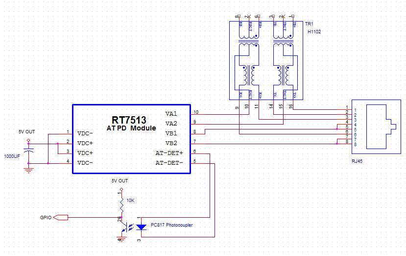
- RT7513 Typical Connection Diagram:
-
- RT7513 Product Selector
Part Number
Nominal Output
Maximum Output Power
AT-DET putout
Marking
Package
RT7513-5V
5V
24W
YES
RT7513
DIP
- Power Classification
The RT7513 classification is fixed at Class 4, this means that an IEEE802.3at Type 1 or an IEEE802.3af PSE will default to Class 0. However an IEEE802.3at PSE will recognise the Class 4 as a Type 2 PD.
- AT Detection
The RT7513 has an AT-DET output pin which is used to detect a Two Event Physical Layer classification as described in IEEE802.3at. If required the AT-DET pin can be connected directly to an opto-coupler.
If the RT7513 detects a Two Event Physical Layer classification, the (AT True) switch will close and Opto1 will turn ON. Opto1 will be connected across the isolation barrier and the output collector can be connected to a controller (with a pull-up resistor connected to the controller’s power rail). When Opto1 is ON the collector (output) will be Logic 0, the controller will then know that the PSE is capable of delivering over 15.4W. To complete the protocol the controller should then confirm that it is a Type 2 PD over the Data Link Layer*.
If the RT7513 detects a Single Event Physical Layer classification, Opto1 will be OFF and the output collector will be Logic 1 (via pull-up resistor). The controller should then assume that the PSE is limited to delivering up to 15.4W.
If the PSE does not support the Physical Layer classification, Opto1 will be OFF. The RT7513 will operate with non IEEE802.3at compliant POE+ PSE’s.
*Note: There are several PSEs (including Cisco) that will only delivery ≤15.4W until they receive Type 2 PD confirmation, over the Data Link Layer.
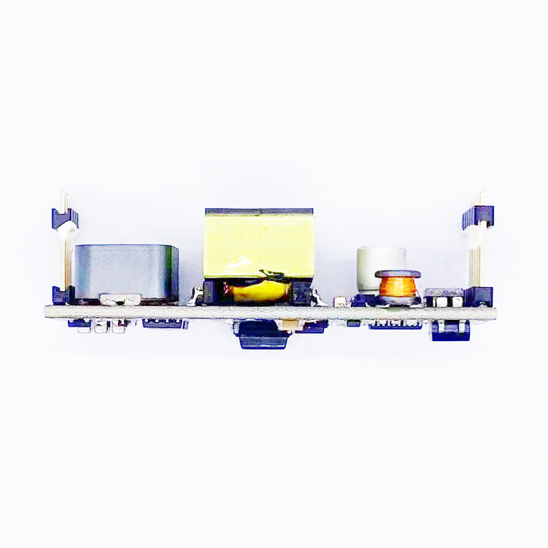
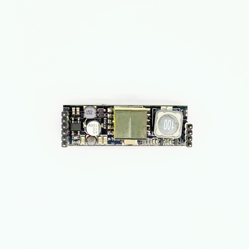
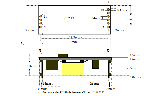
- Package Size: (mm ±3mm )
-
- Pin Description:
Pin
Name
Description
J1
1
-VDC
DC Return. This pin is the return path for the +VDC output.
2
+VDC
DC Output. This pin provides the regulated output from the DC/DC converter.
3
+VDC
DC Output. This pin provides the regulated output from the DC/DC converter.
4
-VDC
DC Return. This pin is the return path for the +VDC output.
J2
5
AT-DET-
AT Detect Output-. Integrated series 5.1 K resistance ,This pin indicates if an IEEE802.3at PSE is supplying power
6
AT-DET+
AT Detect Output+ 10V voltage.
7
VB2
Direct Input (2). This input pin is used in conjunction with VB1 and connects to pin 7 & 8 of the RJ45 connector - it is not polarity sensitive.
8
VB1
Direct Input (1). This input pin is used in conjunction with VB2 and connects to pin 4 & 5 of the RJ45 connector - it is not polarity sensitive.
9
VA2
RX Input (1). This input pin is used in conjunction with VA1 and connects to the centre tap of the transformer connected to pins 1& 2 of the RJ45 connector (RX) - it is not polarity sensitive.
10
VA1
TX Input (2). This input pin is used in conjunction with VA2 and connects to the centre tap of the transformer connected to pins 3& 6 of the RJ45 connector (TX) - it is not polarity sensitive.
-
- Reliability MTBF:
About the life time ,we design according to the following:
1) life time of RT7513 : 100,000 hours @ 25°C
- Safety test items & test report
Test Requested
Test result
Electric strength -1500Vrms at 50 to 60Hz for 60s, applied as specified in subclasuse 5.2.2 of IEC 60950
Pass
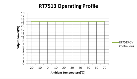
- Operating temp profile
-
- Mechanical / Environmental Performance data
Mechanical / Environmental Performance data
Item
Requirement and Standard
1
Resistance to Wave Soldering Heat
max Preheat Temp range & time 120 ℃ / 180S
max soldering temp &time:265 ℃ / 4S2
Solder ability
Solder able area shall have minimum of 95% solder coverage.
And then into solder bath,Temperature at 245 ±5 ℃ , for 4-5sec.3
Hand Soldering Temperature Resistance
T > =350 ℃ , 3sec at least.
4
Thermal Shock
subject to follow condition for 5 cycles.1 cycles:
-55 ℃ , 30 minutes
+85 ℃ , 30 minutes5
Humidity(Temp Cycling)
less than 95% (non-condensing) ( -20 to 70 ℃)
6
Temperature Life
temperature life at 85℃ for 96 hours.
7
Salt Spray
connectors to 5% salt-solution concentration, 35 ℃
Gold flash for 8 hours there will be no change in the gold layer- Packaging type & Quantity
1.EPE Packaging, 2.Blister Packaging,
60pcs/ dish 50pcs/ dish
480pcs/box 500pcs/box


